News
Neutral Beam Etching System (NBE): Low-Damage Etching Technology for Semiconductor Applications
At SPP Technologies, we are excited to introduce our latest innovation: the Neutral Beam Etching System (NBE). This cutting-edge technology provides low-damage etching solutions for the semiconductor industry, offering significantly reduced damage compared to traditional plasma etching systems.
What is Neutral Beam Etching (NBE)?
Neutral Beam Etching (NBE) technology is an advanced microfabrication technique invented by Professor Seiji Samukawa of National Yang Ming Chiao Tung University (NYCU). He developed this cutting-edge technology during his tenure at Tohoku University before transferring to NYCU.
The application of NBE technology to next-generation devices has been actively researched and developed over the past five years at the Joint Research Center established between Tohoku University and NYCU. This collaboration has resulted in numerous research findings that have been published in various scientific journals.
In August 2022, when Professor Samukawa moved to NYCU, the research began focusing on industrialization in Taiwan. The development process has been informed by input from leading local semiconductor device manufacturers, with the goal of bringing this revolutionary low-damage etching technology to the Taiwanese market.
Usefull Link:
3.5 × 3.5 μm2 GaN blue micro-light-emitting diodes with negligible sidewall surface nonradiative recombination
Key Features of the Neutral Beam Etching System (NBE)
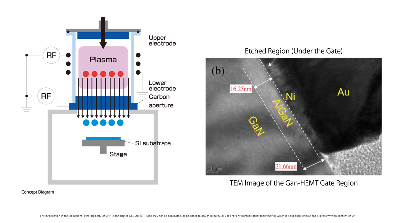
Source of ‘Etched Region‘: Enhancing the Performance of E-Mode AlGaN/GaN HEMTs With Recessed Gates Through Low-Damage Neutral Beam Etching and Post-Metallization Annealing
1. Minimized Plasma Damage
The Neutral Beam Etching System effectively reduces plasma etching damage compared to conventional systems. Its advanced technology ensures minimal device degradation, making it ideal for high-precision applications.
2. Innovative Ion and UV Light Shielding
Featuring a specialized hardware mechanism to block harmful ions and UV light generated during the etching process, the NBE ensures cleaner etching with significantly lower damage to sensitive materials.
Applications of the Neutral Beam Etching System
The Neutral Beam Etching System is designed for a variety of advanced semiconductor applications, delivering outstanding performance in the following areas:
1. High-Frequency HEMT Devices, GaN-HEMT
Ideal for GaN-based HEMT (High Electron Mobility Transistor) devices, the NBE offers unparalleled precision for etching high-frequency components used in cutting-edge technologies.
2. Light-Receiving Devices
The NBE ensures low-damage etching for light-receiving devices, maintaining high signal integrity and reliability for sensitive applications.
3. Light-Emitting Devices, including Micro-LEDs
With its exceptional etching capabilities, the NBE is perfect for enhancing micro-LEDs, enabling high-brightness applications with minimal material damage.
4. LSI CFET
The Neutral Beam Etching System excels in LSI CFET (Complementary FET) processes, offering precision etching for complex, high-performance semiconductor structures.
SPP Technologies’ Collaboration with National Yang Ming Chiao Tung University (NYCU)
In collaboration with National Yang Ming Chiao Tung University (NYCU) in Taiwan, SPP Technologies is working on advancing low-damage etching technology through the Neutral Beam Etching System. This partnership is part of an international joint laboratory with Tohoku University, focusing on materials science and semiconductor technology. Together, we are addressing urgent challenges for a sustainable and smart society, building an academic foundation to solve complex issues in the semiconductor industry.
Through this joint lab, we aim to enhance the NBE’s capabilities, enabling groundbreaking advancements in etching technology for the semiconductor sector.
For more details about the collaboration and our Neutral Beam Etching System, please read the full press release: Joint Development Agreement with National Yang Ming Chiao Tung University in Taiwan – Press Release
Conclusion
The Neutral Beam Etching System (NBE) from SPP Technologies is a revolutionary etching system that ensures low-damage, high-precision etching for advanced semiconductor applications. With its innovative shielding technology and superior etching performance, the NBE is designed to meet the evolving needs of industries relying on precise, super-low-damage etching processes.
To learn more about how the Neutral Beam Etching System can enhance your production processes, and to stay updated on our latest innovations, visit our press release and contact us today.
Stay Ahead of the Competition – Contact Us for More Information About the Neutral Beam Etching System!”

Contact About Equipment
+81 6-6489-5997
Get Product Support
+81 6-6489-5848

Have questions or need assistance?
Get in touch via email.